Google unveiled the Pixel 7 series last week, but didn’t share detailed specs on the new Tensor G2 chipset. Previous rumors indicated a 4nm manufacturing process, but apparently the new SoC is based on a 5nm process, a Google spokesperson confirmed. Android authority.

We don’t receive official confirmation if the Tensor G2 is based on Samsung’s 5LPE process like the Tensor G1 or the newer 5LPP process. Confirmed specs for the Tensor G2 CPU include 2x Cortex-X1, 2x A78 and 4x A55 cores along with clock speed upgrades while the GPU is a Mali-G710 MC10.
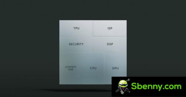
Google Tensor G2 chipset architecture
While a 5nm chipset may not provide the same power efficiency as a 4nm chipset, Google’s new Tensor Processing Unit (TPU) is marketed to offer better power efficiency and to handle the camera and machine learning tasks of the 60’s. % faster than the TPU of the Tensor G1.


Start a new Thread